

In our earlier article about the production cycle of solar panels we provided a general outline of the standard procedure for making solar PV modules from the second most abundant mineral on earth – quartz.
In chemical terms, quartz consists of combined silicon-oxygen tetrahedra crystal structures of silicon dioxide (SiO2), the very raw material needed for making solar cells.
The production process from raw quartz to solar cells involves a range of steps, starting with the recovery and purification of silicon, followed by its slicing into utilizable disks – the silicon wafers – that are further processed into ready-to-assemble solar cells.
Only a few manufacturers control the whole value chain from quartz to solar cells. While most solar PV module companies are nothing more than assemblers of ready solar cells bought from various suppliers, some factories have at least however their own solar cell production line in which the raw material in form of silicon wafers is further processed and refined.
In this article, we will explain the detailed process of making a solar cell from a silicon wafer.
Solar Cell production industry structure
In the PV industry, the production chain from quartz to solar cells usually involves 3 major types of companies focusing on all or only parts of the value chain:
1.) Producers of solar cells from quartz, which are companies that basically control the whole value chain.
2.) Producers of silicon wafers from quartz – companies that master the production chain up to the slicing of silicon wafers and then sell these wafers to factories with their own solar cell production equipment.
3.) Producers of solar cells from silicon wafers, which basically refers to the limited quantity of solar PV module manufacturers with their own wafer-to-cell production equipment to control the quality and price of the solar cells.
For the purpose of this article, we will look at 3.) which is the production of quality solar cells from silicon wafers.
How are silicon wafers made?
Before even making a silicon wafer, pure silicon is needed which needs to be recovered by reduction and purification of the impure silicon dioxide in quartz.
In this first step, crushed quartz is put in a special furnace, and then a carbon electrode is applied to generate a high-temperature electric arc between the electrode and the silicon dioxide.
That process, called carbon arc welding (CAW), reduces the oxygen from the silicon dioxide and produces carbon dioxide at the electrode and molten silicon.
This molten silicon is 99% pure which is still insufficient to be used for processing into a solar cell, so further purification is undertaken by applying the floating zone technique (FTZ).
During the FTZ, the 99% pure silicon is repeatedly passed in the same direction through a heated tube. This process pushes the 1% impure parts to one end, with the remaining 100% pure parts remaining on the other side. The impure part can then be easily cut off.
Crystal seeds of silicon are in the so-called Czochralski (CZ) process put into polycrystalline silicon melt of the Czochralski growth apparatus. By extracting the seeds from the melt with the puller, they rotate and form a pure cylindrical silicon ingot cast out from the melt and which is used to make mono-crystalline silicon cells.
In order to make multi-crystalline silicon cells, various methods exist:
1.) heat exchange method (HEM)
2.) electro-magneto casting (EMC)
3.) directional solidification system (DSS)
DSS is the most common method, spearheaded by machinery from renowned equipment manufacturer GT Advanced. By this method, the silicon is passed through the DSS ingot growth furnace and processed into pure quadratic silicon blocks.
During the casting of the ingots, the silicon is often already pre-doped before slicing and selling the wafer disks to the manufacturers. Doping is basically the process of adding impurities into the crystalline silicon wafer to make it electrically conductive.
These positive (p-type) and negative (n-type) doping materials are mostly boron, which has 3 electrons (3-valent) and is used for p-type doping, and phosphorous, which has 5 electrons (5-valent) and is used for n-type doping. Silicon wafers are often pre-doped with boron.
Once we have our ingots ready, they can then – depending on the geometrical shape requirements, for solar cells usually space-saving hexagonal or rectangular shapes- be sliced into usually 125mm or 156mm silicon wafers by using a multiwire saw.
Processing of silicon wafers into solar cells
The standard process flow of producing solar cells from silicon wafers comprises 9 steps from a first quality check of the silicon wafers to the final testing of the ready solar cell.
Step 1: Pre-check and Pretreatment
The raw silicon wafer disks first undergo a pre-check during which they are inspected on their geometric shape and thickness conformity and on damages such as cracks, breakages, scratches, or other anomalities.
Following this pre-check, the wafers are split and cleaned with industrial soaps to remove any metal residues, liquids or other production remains from the surface that would otherwise impact the efficiency of that wafer.
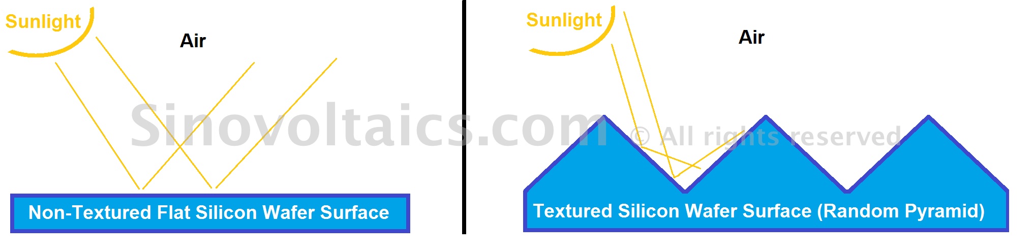
Light reflection difference between a non-textured flat silicon wafer surface and a silicon wafer surface with a random pyramid texture
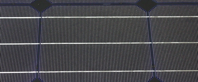
Step 2: Texturing
Following the initial pre-check, the front surface of the silicon wafers is textured to reduce reflection losses of the incident light.
For monocrystalline silicon wafers, the most common technique is random pyramid texturing which involves the coverage of the surface with aligned upward-pointing pyramid structures.
This is achieved by etching and pointing upwards from the front surface. The proper alignment of the pyramids etched out is a result of the regular, neat atomic structure of monocrystalline silicon.
The regular, neat atomic structure of monocrystalline silicon also benefits the flow of electrons through the cell as with fewer boundaries electrons flow much better. Therefore, monocrystalline silicon has an electrochemical structural advantage offering more efficiency over the grainy atomic structures of multi-crystalline silicon.
Now, with such a pyramid structure in place, the incident light does not reflect back and gets lost in the surrounding air but bounces back onto the surface.
Another, less common texturing technique is the inverted pyramid texturing. Instead of pointing upwards from the front surface, the pyramids are etched into the wafer’s surface, similarly achieving reflection losses of incident light trapped in the inverted pyramid holes.
The texturing of multi-crystallin silicon wafers requires photolithography – a technique involving the engraving of a geometric shape on a substrate by using light – or mechanical cutting of the surface by laser or special saws.
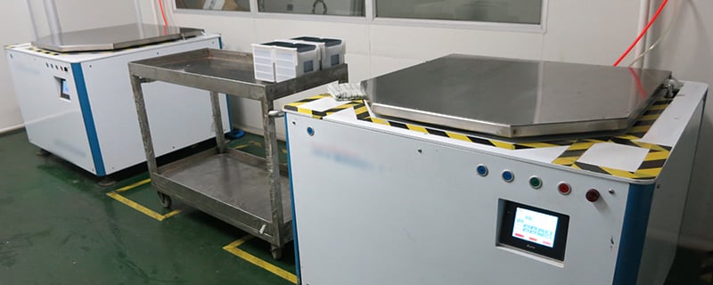
Step 3: Acid Cleaning
After texturing, the wafers undergo acidic rinsing (or: acid cleaning). In this step, any post-texturing particle remains are removed from the surface.
Using hydrogen fluoride (HF) vapor, oxidized silicon layers on the substrate can be etched away from the wafer surface. The result is a wet surface that can be easily dried.
By using hydrogen chloride (HCl), metallic residues on the surface can be absorbed by the chloride and thus removed from the wafer.
Step 4: Diffusion
Diffusion is basically the process of adding a dopant to the silicon wafer to make it more electrically conductive. There are basically 2 methods of diffusion: solid-state diffusion and emitter diffusion.
While the former method basically involves the already mentioned uniform doping of the wafers with the p-type and n-type materials, the emitter diffusion refers to the placing of a thin dopant material-containing coating on the wafer bypassing the wafers through a diffusion coating furnace.
Wafers that have already been pre-doped with p-type boron during the casting process are during the diffusion process given a negative (n-type) surface by diffusing them with a phosphorous source at a high temperature, creating the positive-negative (p-n) junction.
Why diffuse the wafers though? This junction of electron deficiency in the p-type and high electron concentration in the n-type allows for excess electrons from the n-type to pass to the p-type, a flow creating an electron field at the junction.
Step 5: Etching & Edge Isolation
During diffusion, the n-type phosphorous diffuses not only into the desired wafer surface but also around the edges of the wafer as well as on the backside, creating an electrical path between the front and backside and in this way also preventing electrical isolation between the two sides.
The objective of the etching and edge isolation process is to remove this electrical path around the wafer edge by disk stacking the cells on top of each other and then exposing them to a plasma etching chamber using tetrafluoromethane (CF4) to etch exposed edges.
Step 6: Post-Etching Washing
After the etching, particle residues' potential remains on the wafer and the wafer edges. Therefore the wafers need to undergo a second washing to remove the remains of the previous etching process.
After this second washing, the wafers can further be processed for the deposition of anti-reflective (AR) coating.
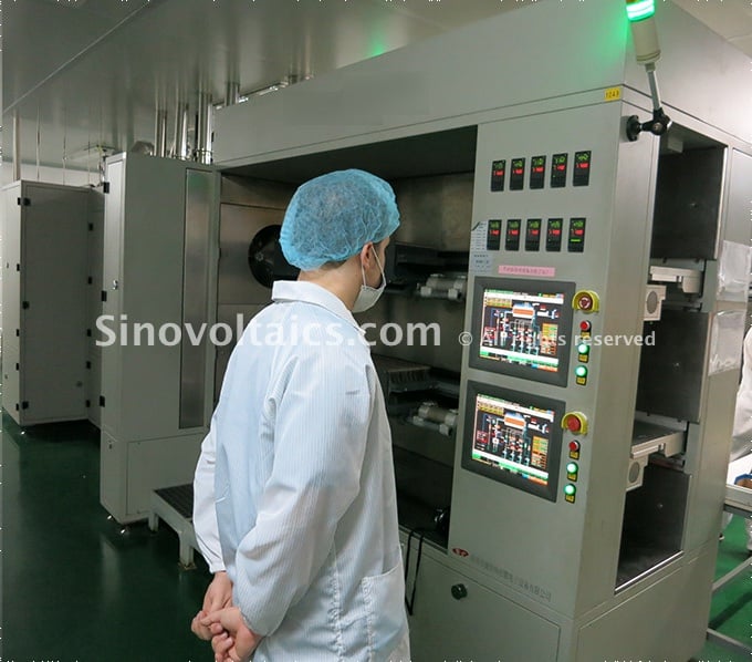
Niclas checking cell production at a PEVCD machine
Step 7: Anti-Reflective Coating Deposition
In addition to surface texturing, AR coating is often applied on the surface to further reduce reflection and increase the amount of light absorbed into the cell.
This anti-reflective coating is very much needed as the reflection of bare silicon solar cells is over 30%. For the thin AR Coating, silicon nitride (Si3N4) or titanium oxide (TiO2) is used. The color of the solar cell can be changed by varying the thickness of the anti-reflection coating.
In the semiconductor industry, there are basically three methods to depose layers on wafers, which are:
1.) Atmospheric Pressure Chemical Vapor Deposition (APCVD), which is used only for a few applications and requires high temperatures.
2.) Low-Pressure Chemical Vapor Deposition (LPCVD), which involves the deposition process to be performed in tube furnaces and like the APCVD method requires high temperatures.
3.) Plasma Enhanced Chemical Vapor Deposition (PECVD), which is the most common method for the deposition of AR coating on the wafer.
In the PECVD process, the thin coating exists in a gaseous state and is through a chemical reaction process solidified onto the wafer.
Step 8: Contact Printing and Drying
As the next step, metal inlines are printed on the wafer with the objective to create ohmic contacts. These metal inlines are printed on the rear side of the wafer, which is called backside printing.
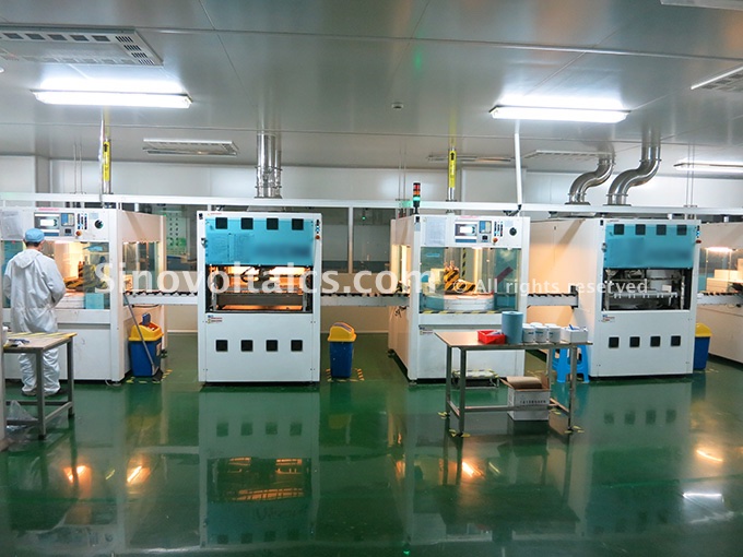
Contact Printing and Drying Machinery
This is achieved by printing the metal pastes with special screen printing devices that place these metal inlines onto the backside. After printing, the wafer undergoes a drying process.
Once dry, this process is followed by the printing of the front side contacts, then the wafer is another time dried.
After all, contacts have been printed on the rear and front sides, the screen-printed wafers are passed through a sintering furnace to solidify the dry metal pastes onto the wafers. Then, the wafers are cooled and can already be called solar cells.
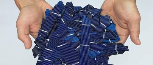
Step 9: Testing and Cell Sorting
In this final process, the now ready-to-assemble solar cells are tested under simulated sunlight conditions and then classified and sorted according to their efficiencies.
This is handled by a solar cell testing device that automatically tests and sorts the cells. The factory workers then only need to withdraw the cells from the respective efficiency repository to which the machine assorted the cells.
The solar cell then basically becomes a new raw material that is then used in the assembly of solar PV modules. Depending on the smoothness of the production process and the basic silicon wafer material quality, the final outcome in form of a solar cell is then further graded into different solar cell quality grades.
TO OUR READERS:
In this article we went through the standard production process from silicon wafer to solar cells. However, there are many quality problems that can potentially be created early on in this process. Which potential quality risks are you aware of when processing silicon wafers into solar cells? If you are aware of potential quality problems or have experience in solar cell production, we kindly invite you to share more insights with the Sinovoltaics Community!

Olivia Davis
on 07 Aug 2023Saikiran
on 07 May 2023VIJYOT POWER
on 01 Oct 2022Obed Maringa
on 17 Aug 2023Rakip Rahangdale
on 23 May 2022Khalid Alweli
on 11 Aug 2021Ashok
on 30 Jun 2019Rebecca
on 25 Jan 2019Abdul Jabbar
on 25 Oct 2018Shashikant singh
on 30 Jan 2018Uday chitre
on 26 Jan 2018Dinesh Soni
on 09 Nov 2017aayun tanwar
on 03 Nov 2017Hussein
on 11 Jul 2017khouloud jaffel
on 24 May 2017