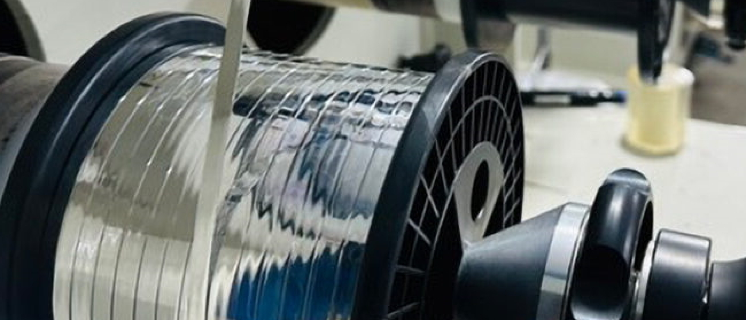
Bussing Ribbons: Design and Purpose
Bussing ribbons employed in the photovoltaic panels are a part of the arrangement for collecting energy from the cell and conveying it over two line to a junction box. The junction box can feed an inverter or other loads.
PV Current Collection
A solar cell will produce a uniform density of current all over its surface when irradiated by sunlight. The current must be collected from all over the cell and conveyed to the junction box. The cell size is, as a standard practice is 6in by 6in. We cannot place a copper contact covering the whole surface, because that will deprive the cell of the entire sunlight and there will be nothing to collect. We must collect from the entire surface causing minimum shading over the cell area. The solution that has evolved is fine parallel conducting fingers all over the surface, intercepted by conducting bus bars at right angles which collect from the fingers. The bus bars are soldered with tabbing ribbon conductors. The bus bars are then bussed together to collect their currents on one conductor called the bussing ribbons. The bussing ribbons lead to the junction box.
Bussing Ribbons
Flatt copper conductors similar to tabbing ribbons but wider (5 mm wide) with pre-soldered surfaces are used to run across the bus bars collecting their current just as bus bars run across fingers to collect their currents. Like tabbing ribbon bus ribbons are also made from “oxygen-free high conductivity” (OFHC) copper (OFHC) copper. A solid round conductor is rolled precisely to obtain a flat ribbon conductor about 0.2 mm thick. The ribbon surfaces are covered with solder so as to prevent oxidation during transit and storage. The surface may be silver plated to assure better conductivity and reflectivity. Good reflectivity helps mitigate the shading effect of the conductors to some extent. Light reflected by the top surface of the ribbon gets totally internally reflected again at the glass air interface. And most of it becomes available again to the cell for conversion. The solder layer is about 0.025 mm thick. The copper used is “dead soft” so that it can be easily bent for soldering to the cells and after the connection, does not stress the cell.
Factors Critical to Ribbon Design
Except that the bussing ribbons are wider (5mm) than the tabbing ribbons (2 mm) the bussing ribbons are similar to the tabbing ribbons. Parameters contributing to quality of the bussing ribbons are the base material, ductility, camber, yield strength, etc.
