Power Conditioning System
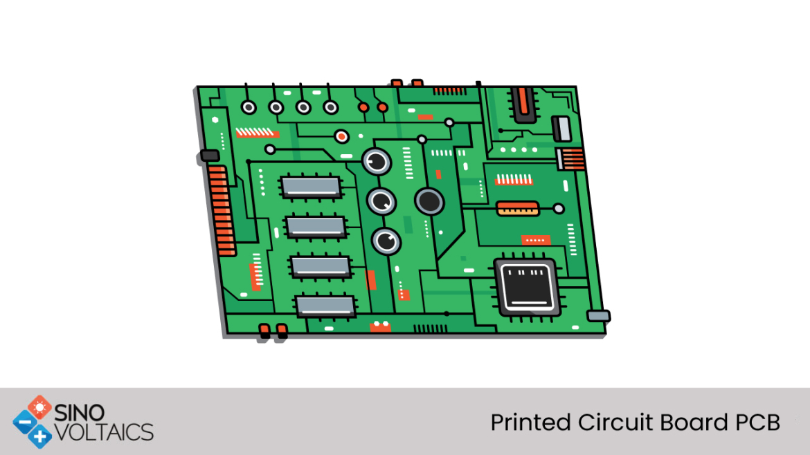
PCB
Connectors without locking device
Connectors with Locking Device
Ingress Protection
Intermateability of Connectors
Solar Glass
Bus Wire and Tab Wire
[...]

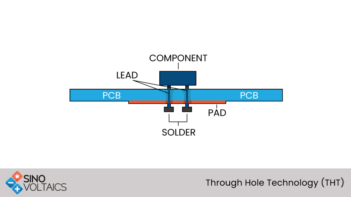
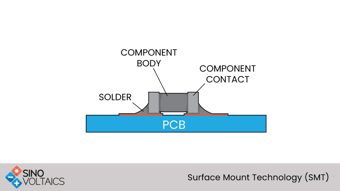 Components can be mounted in two ways. Through hole components are mounted by passing the wire leads through the board and soldering them to traces on the other side. Surface mount components are soldered by their leads to copper traces on the same side of the board.