Albedo
Bypass Diodes
Solar Glazing
Single Phase Versus Three Phase Power Supply
Three phase power supply
Single Phase Power Supply
Module Measurement without Load
Module Measurement with Load
[...]

Variations of number of electrons and holes in a semiconductor can be achieved by a technique called Doping . Doping makes N-type material when a semiconductor material from group IV is doped with atoms from group V. While P-type materials are made when a semiconductor material from group IV is doped with atoms from group III. N-type materials increase the semiconductor’s conductivity by increasing the number of available electrons; while P-type materials increase the semiconductor’s conductivity by increasing available holes number. The balance of electrons and holes in a silicon crystal lattice shifts by doping with other atoms. Atoms that have one more valence electron than silicon are used in production of n-type semiconductor material. These n-type materials are elements of group V in the periodic table, and therefore their atoms contain 5 valence electrons that can form covalent bonds with the 4 valence electrons that the silicon atoms have. Since only 4 valence electrons from each atom are required from n-type and silicon to form the covalent bonds around the silicon atoms, the extra valence electron existing (since there are 5 valence electrons in n-type materials) when the two atoms bond, which is free to join in conduction. Consequently, the conduction band has more electrons added to it and therefore increasing the number of present electrons.
Atoms that have one less valence electron are used in p-type material. These p-type materials are elements of group III in the periodic table. So, p-type material can interact with silicon atoms with only the available 3 valence electrons. This ultimately results in a hole, as the available electrons are not enough to form the 4 covalent bonds around the atoms. The number of electrons in p-type material trapped in bonds is higher, thus leading to increase in the number of holes There is always more of a single type of carrier than the other in doped material, where majority carrier is the type of carrier with higher concentration while minority carrier is the type of carrier with the lower concentration. A summary of the properties of semiconductor types in silicon is in the following below: 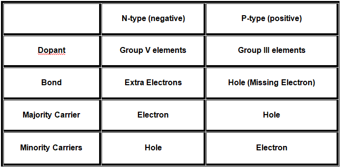 There could be around 1017cm-3 majority carriers and 106cm-3 minority carriers in a typical semiconductor. Stated differently, the ratio of minority to majority carriers is less than one to the entire planet’s population. Minority carriers can be created in two ways, thermally or by incident photons. N-type semiconductor are called n-type because the majority carriers are Negatively charged electrons. While P-type semiconductor are called p-type because the majority carriers are positively charged holes.