Degradation of Solar Cell Performance Due To Microcracks
CZTS Solar Cells
Float Zone Silicon Cells (FZ)
Different Wafer Sizes
Photoelectrochemical Cell
CIGS solar cells
Luminescent Solar Concentrator Cells
Solid State Solar Cells
[...]

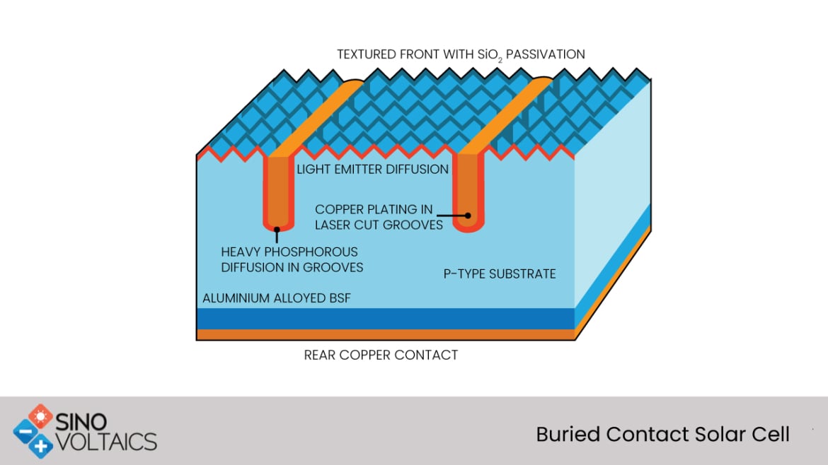 The buried contact technology allows for lower parasitic resistance losses as well because of high metal aspect ratio, the fine finger spacing and the contacts plated metal. The emitter resistance is decreased in the buried contact solar cell because the narrower finger spacing decreases the emitter resistance losses dramatically. The metal grid resistance is low as well because the finger resistance is reduced by the large metal volume in the grooves and by the copper use, as it has lower resistivity than the metal paste used in screen printing. Also, the contact resistance of the buried contact solar cell is less than that of screen printed solar cells as a result of the formation of nickel silicide at the interface of semiconductor metal and the large metal-silicon contact area. Overall, the reduced resistive losses leads to larger area solar cells with high Fill Factors.
When compared to screen printed solar cell, the metalization structure of a buried contact solar cell improves emitter of the cell as well. The emitter region of the screen printed solar cell is doped very heavily and leads to a dead layer at the solar cell’s surface. Based on low emitter losses in the buried contact structure, the emitter doping can be optimized for short-circuit currents and high open-circuit voltages. Adding to that, a buried contact structure has a self aligned selective emitter, which also reduces the contact recombination and contributes as well to high open circuit voltages.
The buried contact technology allows for lower parasitic resistance losses as well because of high metal aspect ratio, the fine finger spacing and the contacts plated metal. The emitter resistance is decreased in the buried contact solar cell because the narrower finger spacing decreases the emitter resistance losses dramatically. The metal grid resistance is low as well because the finger resistance is reduced by the large metal volume in the grooves and by the copper use, as it has lower resistivity than the metal paste used in screen printing. Also, the contact resistance of the buried contact solar cell is less than that of screen printed solar cells as a result of the formation of nickel silicide at the interface of semiconductor metal and the large metal-silicon contact area. Overall, the reduced resistive losses leads to larger area solar cells with high Fill Factors.
When compared to screen printed solar cell, the metalization structure of a buried contact solar cell improves emitter of the cell as well. The emitter region of the screen printed solar cell is doped very heavily and leads to a dead layer at the solar cell’s surface. Based on low emitter losses in the buried contact structure, the emitter doping can be optimized for short-circuit currents and high open-circuit voltages. Adding to that, a buried contact structure has a self aligned selective emitter, which also reduces the contact recombination and contributes as well to high open circuit voltages.