Electroluminescence
What is Electroluminescence?
Electroluminescence is the optical and electrical phenomenon where a specific material emits light as a result of the passage of an electric current through it. Electroluminescence shares the same concept as the LED ( light emitting diode). Current flows into the solar cell which basically acts as a large diode, then radiative recombination of carriers causes light emission. For the indirect bandgap semiconductor, the majority of recombination in silicon occurs due to defects or Auger recombination. The percentage of band-to-band recombination which produces radiative emission is comparatively low. Yet, there is still a small quantity of radiative recombination that occur even in silicon and this signal can be detected using an external sensor. This technique requires electrical contact and thus can only be used after the metallization has been applied to the cell and the cell is substantially complete. Electroluminsecence provides a lot of important data about the area related uniformity of solar cells or modules. It is a non destructive technique and fairly fast with possible measurement time of 1 second.
Mechanism
Electroluminescence is the outcome of the radiative recombination of holes & electrons in the semiconductor material. The excited electrons discharge their energy as photons (light). Before recombination, electrons and holes can be separated by either doping of the material to form a pn junction (in the semiconductor electroluminescent equipment such as light emitting diodes) or through excitation by impact of high energy electrons that are accelerated by a strong electric field (like the phosphors in electroluminescent displays).
Electroluminescence Detectors
Electroluminescence detectors have become more and more popular with the advancement of low cost CCD silicon arrays. They are identical to the ones used in digital cameras but with optimization for sensitivity in the near-infrared and cooled to reduce the thermal noise. Similar to the digital cameras, there are detectors with multiple mega pixels resolution of 2048 * 4096 pixels which enables high resolution images for the entire modules. One of the significant drawbacks of a silicon detector is that they have a poor response beyond 1000 nm level because of the low absorption coefficient of silicon. An alternative detector to silicone is the InGaAs photodiodes array, which has a much higher response over the 1000 to 1300 nm wavelength range thus enabling a much faster data acquisition rate but with a considerably higher cost. Resolution typically is in the sub-megapixel range with 640 × 512 pixels as the most common.
Images
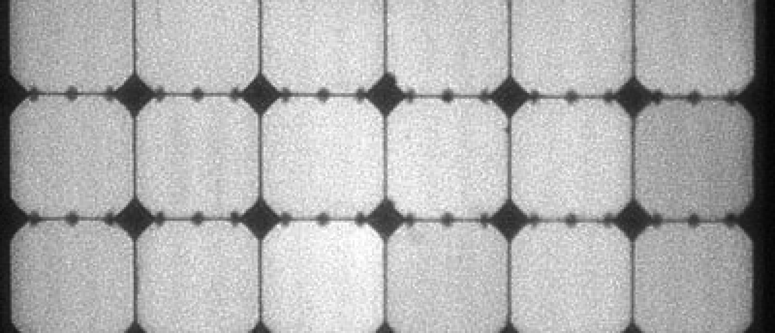
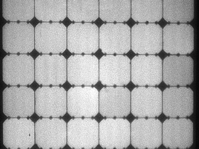
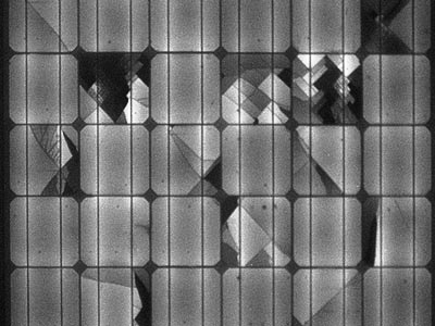
The key advantage as highlighted before is the ability of electroluminescence imaging for the complete solar cell or module in a comparatively short space of time. The light output increases as the local voltage increases, so poor contact regions show up as dark regions. This technique is used by the El Tester for identifying all quality problems for the manufactured solar cells.
 Quality Cells
 Defect Cells
ELCD Test: what is it and purpose?
With the help of an ELCD test (ELCD: electroluminescence crack detection), a PV manufacturer can evaluate the structural quality of solar cells and any other possible defects caused by improper handling of photovoltaic panels. Nowadays the majority of large solar panel manufacturers have integrated the ELCD test in their production lines. At the same time, many small and medium sized manufacturers do not invest in ELCD test equipment.
